AI Dynamics

Global AI News Aggregator

About

HARDWARE

  • llama.cpp achieves 300 tokens/second on Mac Studio M2 Ultra

    Let me demonstrate the true power of llama.cpp: – Running on Mac Studio M2 Ultra (3 years old) – Gemma 4 26B A4B Q8_0 (full quality) – Built-in WebUI (ships with llama.cpp) – MCP support out of the box (web-search, HF, github, etc.) – Prompt speculative decoding The result: 300t/s (realtime video)

    → View original post on X — @julien_c, 2026-04-02 17:11 UTC

  • MLPerf Power Selected for IEEE MICRO Top Picks 2025
    MLPerf Power Selected for IEEE MICRO Top Picks 2025

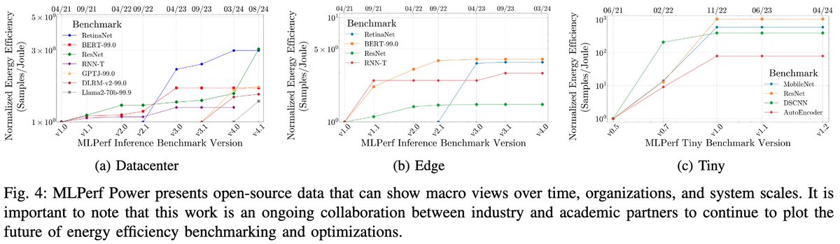
    Super excited to share that MLPerf Power (HPCA 2025) was selected for IEEE MICRO Top Picks 2025, 1 of the 12 most impactful computer architecture & systems papers of the year! Power consumption is the defining constraint for modern ML systems. Microsoft, Google, Amazon, Meta, and OpenAI have all announced plans for gigawatt-scale datacenters (for context, 5 GW = 5 nuclear reactors = Miami's power footprint). On the other end of the spectrum, we're anticipating billions of AI-enabled devices at the edge. We created MLPerf Power to be the industry-standard to measure, understand, and compare energy use across all deployment scales. We're excited to see that it's already impacting individual companies' strategies and has been incorporated into the IEEE semiconductor roadmap. We @MLCommons also collect and open source over 1,800 reproducible measurements from 60 diverse systems. These reveal several important insights that shed light on the nonlinear scaling of energy efficiency in modern systems and can enable many new data-driven optimization approaches. Just as @MLPerf aligned industry towards shared performance goals, we are hopeful that MLPerf Power will do the same for power and energy efficiency!

    → View original post on X — @askalphaxiv, 2026-04-02 17:00 UTC

  • Melody: AI-Powered Multilingual Humanoid Girlfriend Robot

    Meet Melody—The #AI-Powered, Multilingual Humanoid Girlfriend
    by @MarioNawfal #Robotics #Technology #ArtificialIntelligence #MI #ML #Innovation

    → View original post on X — @ronald_vanloon

  • Gemma4 vindicated: dense models triumph over mixture of experts
    Gemma4 vindicated: dense models triumph over mixture of experts

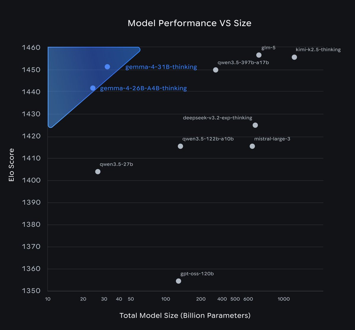
    Gemma4 is amazing. You'll read that everywhere. Let's focus on what is HUGE here: the revenge of dense models…. Throw away your b200, not needed anymore, throw away the millions of lines of code we had to write to make MOEs faster, training stable etc… throw away your router-aware kernel, your EP DEEP GEMM, throw away the auxiliary loss function. Welcome to simplicity, dense is the new king. FINALLY hating MoEs is back to being chad. For those who know me: I was always a moe doomer

    → View original post on X — @jeremyphoward, 2026-04-02 16:23 UTC

  • Google Gemma 4 Now Available on Modular Cloud Platform

    Google Deep Mind's impressive fully-open Gemma 4 is live day-zero on Modular Cloud. Modular provides the fastest performance on NVIDIA Blackwell and AMD MI355X, thanks to MAX and Mojo🔥. The team took this impressive new model to production inference in days.🚀

    → View original post on X — @jeremyphoward, 2026-04-02 16:15 UTC

  • Semiconductor Yield Problem Solved by Cerebras Wafer Scale Processors
    Semiconductor Yield Problem Solved by Cerebras Wafer Scale Processors

    What is semiconductor yield? How does it work? Why did it define the semiconductor industry for 70 years? How did this problem get solved? And how does this impact developers? What Is Semiconductor Yield? When you manufacture chips, not every one comes out working. Some have defects. “Yield” is the percentage of chips from a manufacturing run that actually work. If you make 100 chips and 90 work, your yield is 90%. How Does Yield Work? Chips are made from silicon wafers – thin, circular discs about 12 inches in diameter. In a perfect world, every square millimeter of a wafer would be flawless. But that never happens. Every wafer has tiny random defects scattered across it. Chips are cut from these wafers. And any chip that lands on a defect is thrown away. The process of chip manufacturing looks a lot like your mother making cookies. Imagine your mom rolled out a circle of cookie dough 12 inches in diameter. Then when she wasn't looking, your brother threw a handful of peanut M&Ms into the air and they landed at random on the dough. Those M&Ms are flaws. Nobody can eat a cookie with a peanut M&M in it. So she has to throw away every cookie that has one. Now she gets out a small cookie cutter and stamps out cookies. Because the cookie cutter is small, the probability of hitting an M&M is low. And when a cookie does have one, there isn't much good dough surrounding it. Not much good dough is thrown away. The result: a lot of good cookies. They are small but there are a lot of them. On the other hand, if she uses a big cookie cutter, the probability of hitting an M&M is much larger. And when she throws that cookie away, she throws away a lot of good dough with it. The result: only a few cookies. They are big, but the 12 inch diameter circle of dough yielded only a few. This is exactly how chip manufacturing works. The cookie dough is a silicon wafer. The cookies are chips. Peanut M&Ms are flaws (because they are gross) Bigger chips hit more flaws. More good silicon gets thrown away. Smaller chips, like smaller cookies, are less likely to hit flaws. And when they do, less silicon is discarded. This is why big chips are disproportionately more expensive. This is also why people assumed that because there was no way to make a wafer without flaws, there was no way to make a chip the size of a wafer. Why Did This Define The Industry For 70 Years? In an ideal world, you'd build really big chips for many data center applications. Data moves incredibly fast on-chip. So if you keep the data and compute on-chip, your work takes less time, and uses less power. In AI, that manifests as super fast inference. But the moment data has to leave one chip and travel to another – through cables, switches, connectors, circuit boards – it slows down and uses more power. Lots of off-chip communication slows work, and, in AI, produces slow inference. Though everyone agreed they were faster, nobody could yield big chips. So the industry settled on a workaround: don't build one big chip. Build thousands of small ones and wire them together. Most AI data centers are built this way today. Thousands of little GPUs connected by cables, switches, and networks. It works. But you pay a price. Every connection adds latency. Every cable adds overhead. Every hop between chips slows things down. For 70 years, everyone accepted this as the only way. How Did Cerebras Solve the Yield Problem? In 2019, we solved the yield problem at @cerebras and brought the first wafer sized processor, wafer scale processor, to market. How did we do that? The answer came from studying a different kind of chip entirely. Memory. Memory is built with a different process. Memory chips are made up of millions of identical tiles, with redundant tiles woven throughout. In a memory chip, if a tile has a flaw in it, the chip doesn't get thrown away. The bad tile is shut down and one of the redundant ones is called into action. Memory chips weren't designed to avoid flaws, but rather to withstand them. They use redundancy to withstand flaws. And their yield is extraordinary. Our founders realized that if we could develop a compute architecture that looked like memory, that was built of hundreds of thousands of identical tiles, we too could use redundancy to withstand flaws. We could fail in place, and route around the failed tile, just as they do in memory (and interestingly as they do in data centers where they fail in place, route around, and keep going). This would enable us to yield a wafer scale processor. And today we are happy to compare our yields to GPUs, that are 1/58th our size. How Does This Impact Developers? The impact is simple and easy to see. Cerebras wafer scale processors are up to 15 times faster than @nvidia GPUs. And when your AI is fast, people use it more often, stay longer, and use it to solve more interesting problems.

    → View original post on X — @cerebras, 2026-04-02 16:07 UTC
  • Gesture-Controlled Racing Game with Hand Tracking Technology
    Gesture-Controlled Racing Game with Hand Tracking Technology

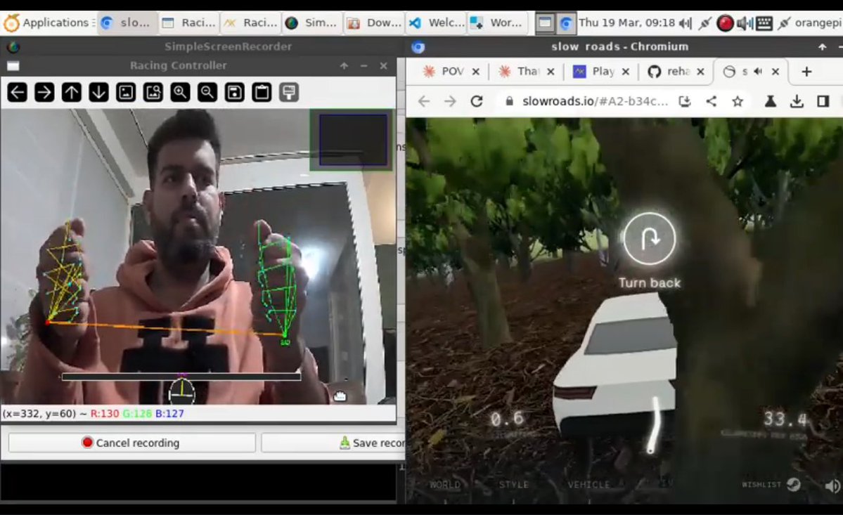
    Gesture-controlled racing, no controller needed. YOLO11n-pose-hands on Metis for 21-keypoint hand tracking. Tilt wrists to steer, fist to accelerate, open palm to brake. Works with any keyboard racing game. Built by Dilip.m. #EdgeAI #Gaming 🏎️ eu1.hubs.ly/H0t1WCm0

    → View original post on X — @axeleraai, 2026-04-02 15:52 UTC

  • Holodeck: Beyond VR Into Immersive Reality

    We will call it the Holodeck. People won’t see it as VR.

    → View original post on X — @scobleizer

  • Smart Humanoid Robot Transforms Home Assistance and Caregiving

    Smart Humanoid #Robot Aims to Transform Home Assistance and Caregiving
    via @ZappyZappy7 #Robotics #ArtificialIntelligence #Innovation #Technology

    → View original post on X — @ronald_vanloon

  • GPU Power Draw as True Utilization Metric in Data Centers

    Without getting all the way down to performance counters, GPU power from nvidia-smi is a better indicator of true utilization than job scheduling or “gpu busy”. I would love to see animated “heat maps” of the big data centers, with each pixel being an individual GPU’s power draw. I am confident that inference and frontier training at the big labs is highly efficient, but I wonder how many GPUs would be dark due to scheduling and inefficient research code. With a little calibration for base load and peak, just the power bill for the datacenter would be a pretty good first order indicator of utilization.

    → View original post on X — @id_aa_carmack, 2026-04-02 14:49 UTC